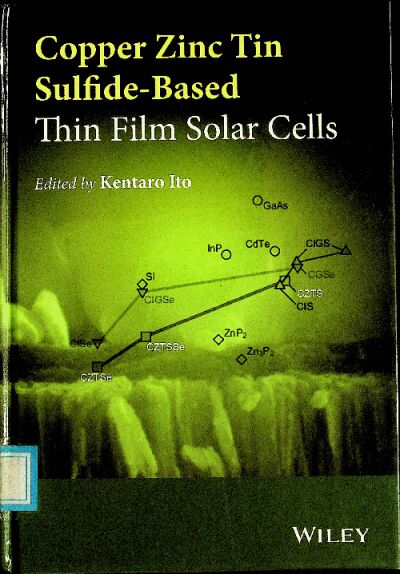
书名:Copper zinc tin sulfide-based thin-film solar cells
责任者:Kentaro Ito | Shinshu University | Nagano | Japan. | Ito, K.
出版时间:2015
出版社:John Wiley & Sons Inc.,
前言
The most cost-effective route to solar cell fabrication was unlocked by utilizing thin-film technology. The first research papers on this type of cell date back to the 1960s. The semi- conductor thin film consisting of a II-VI or 1-111-V12 compound is normally used in the solar cell as an optical absorber with the thickness of microns. It is prepared on a low-cost substrate such as a glass plate, a metal sheet, or a plastic sheet. It was found in the late 1980s that the thin film of quaternary compound Cu2ZnSnS4 also has a suitable energy band and exhibits a photovoltaic effect. In this book we deal with the multinary compound semiconductors which belong to the tetragonal crystal system and have the optimal band gap for photovoltaics: the quaternary sulfide, its alloy, and a selenide. The chemical formu- lae of the latter are represented as Cu2ZnSn(S Se ) and Cu2ZnSnS%. The purpose of this book is to describe current development of thin-film solar cells, from the viewpoint of device performance and absorber processing. We also describe the physical and chemical properties of these compounds, which are considered to play an important role in determin- ing the efficiency of the solar cells.
In the mid-1970s, Professor A. G. Milnes of Carnegie Institute of Technology visited our University in Nagano to speak on the subject of solar cells. At that time he was a visiting scholar at the Tokyo Institute of Technology. He stressed the importance of cost in produc- ing solar cells, and predicted that photovoltaics would not be of any practical use if the cost was higher than the threshold value (equal to ten cents per watt). He made numerous refer- ences to this threshold in his talk. He was interested in developing a low-cost GaAs solar cell which is grown epitaxially on a mono-crystalline substrate, a substrate which could be made reusable by detaching it many times from the epitaxial layer using selective chemical etching. Around that time, the efficiency of a GaAs solar cell was 22% while that of a CdTe thin-film solar cell was 8%. Although his concept is indirectly connected to the recent development of a GaAs solar cell, the efficiency of which has approximately reached the theoretical upper limit, it has not been applied to low-cost solar cells because the large-area mono-crystals are not available. By taking account of the rise in electricity rates (Consumer Price Index) during the past four decades, his threshold has to be upgraded to 45 (54) cents per watt at present. It is interesting to note that this converted threshold is only 1.5 times lower than the price of CdTe thin-film solar modules in 2013, as shown in Chapter 2. Despite polycrystalline nature, cost-effective performances of thin-film solar cells are preferable to those of mono-crystalline solar cells.
Multinary compound semiconductors have an absorption coefficient > 104 cm-l due to the direct nature of the band gap. Films of thickness I Vim can absorb almost all the photons in the solar spectrum of wavelength shorter than near-infrared wavelengths, and operate as efficient photocurrent suppliers. The direct band gap is within an optimal range for solar cells, that is, 1.0—1.5 eV. The theoretical upper limit of efficiency for the solar cells is esti- mated to be 32—34%. There is still room for improvement in the present cell performance via a high-quality absorber layer and the optimization of device structure. Since all the chemical elements of the compound are Earth-abundant, the material cost of the absorber can be much lowered in comparison to the II-VI or 1-111-V12 thin-film solar modules in which the absorbers are composed of rare elements such as Te and In.
For the sake of simplicity, the chemical formulae are often abbreviated by replacing cop- per, zinc, tin, sulfur, and selenium with C, Z, T, S, and Se, respectively, and the suffixes are omitted. Photovoltaic devices which consist of these compounds are referred to as CZTS- based thin-film solar cells. In the first chapter of Part I it is described how the concept for CZTS-based thin-film solar cells is derived from the physical principle of photovoltaics and also from the viewpoint of abundant natural resources. In the second chapter, their prospects are discussed by reviewing recent advances in producing thin-film solar modules, among which CdTe modules exhibit a learning curve pointing at price SUS 0.7 per peak watt.
In the first chapter of Part II, it is described that the principal structure type of CZTS is kesterite, and the existence of some antisite point defects in the compound is demonstrated by neutron diffraction. Relatively small electron mass and high optical efficiency of the multinary compounds are deduced from theoretical studies of the energy band structure and complex dielectric function, respectively. We learn how CZTS is in thermal equilibrium with volatile sulfur and tin sulfide at growth temperatures, and that the existence of second- ary phases in CZTS should be identified using specific analyses. Bulk CZTS single crystals are grown by solution growth, and their transport property is evaluated by Hall measure- ments. Physical properties of Cu -II-IV-V14 compounds are systematically compiled such that their data can provide useful information for the design of thin-film solar cells.
Various processes involved in the preparation of high-quality absorbers for solar cells are introduced in Part Ill. Study of thin-film CZTS solar cells reveals that a Cu-poor and Zn-rich absorber — prepared by sulfurizing a precursor — is required for the improvement of cell effi- ciency. Disordered CZTS thin films are first sputter-deposited from metal targets in a residual vapor pressure of H2S and are then annealed in sulfur vapor. After coevaporation techniques are elucidated to grow thin-film compounds, their application to CZTS-based thin-film solar cells are reviewed. CZTSe thin films are prepared by annealing the precursor in Se vapor, which is formed by coating a substrate with the ink composed of CZTS nanocrystals. CZTS thin films are prepared by oxidation and subsequent sulfurization of an oxyhydrate precursor which is coated by the sol-gel method. Mono-grain crystallites of the CZTS-based compounds are grown by a flux method and they are arranged in a mono-grain layer to make solar cells.
Part IV is on the device physics of thin-film solar cells. According to the microscopic observation by SKPM and conductive AFM, the enhanced minority carrier collection takes place at the grain boundaries of multinary compounds. The efficiency of CZTS-based thin- film solar cells fabricated by coevaporation and annealing is at least partly correlated with the defect density in the absorber. The device characteristics of the thin-film solar cells are reviewed, and the high series resistance in them is considered attributable to such a secondary phase as ZnSe. Using the hydrazine pure-solution approach, a CZTSSe thin-film solar cell with 12.6% efficiency is obtained. The possible effect of band tailing on the open- circuit voltage is discussed.
We are indebted to Ms Sarah Keegan, Ms Emma Strickland and Ms Rebecca Stubbs for their assistance with manuscript preparation.
查看更多
目录
Preface ix
List of Contributors xi
Part I Introduction 1
1 An Overview of CZTS-Based Thin-Film Solar Cells Kentaro Ito 3
1.1 Introduction 3
1.2 The Photovoltaic Effect 4
1.3 In Pursuit of an Optimal Semiconductor for Photovoltaics 22
1.4 Conclusions 36
Acknowledgements 37
References 37
2 Market Challenges for CZTS-Based Thin-Film Solar Cells Arnulf Jager-Waldau 43
2.1 Introduction 43
2.2 Compound Thin-Film Technologies and Manufacturing 45
2.3 Challenges for CZTS Solar Cells in the Market 49
2.4 Conclusion 51
References 51
Part II The Physics and Chemistry of Quaternary Chalcogenide Semiconductors 53
3 Crystallographic Aspects of Cu2ZnSnS4 (CZTS) Susan Schorr 55
3.1 Introduction: What Defines a Crystal Structure? 55
3.2 The Crystal Structure of CZTS 57
3.3 Point Defects in CZTS and the Role of Stoichiometry 68
3.4 Differentiation between Intergrown Kesterite- and Stannite-Type Phases: A Simulational Approach 71
3.5 Summary 72
References 73
4 Electronic Structure and Optical Properties from First-Principles Modeling Clas Persson, Rongzhen Chen, Hanyue Zhao, Mukesh Kumar and Dan Huang 75
4.1 Introduction 75
4.2 Computational Background 77
4.3 Crystal Structure 80
4.4 Electronic Structure 82
4.5 Optical Properties 97
4.6 Summary 101
Acknowledgements 102
References 102
5 Kesterites: Equilibria and Secondary Phase Identification Dominik M. Berg and Phillip J. Dale 107
5.1 Introduction 107
5.2 Chemistry of the Kesterite Reaction 108
5.3 Phase Identification 116
Acknowledgements 128
References 128
6 Growth of CZTS Single Crystals Akira Nagaoka and Kenji Yoshino 133
6.1 Introduction 133
6.2 Growth Process 134
6.3 Properties of CZTS Single Crystals 141
6.4 Conclusion 145
Acknowledgements 146
References 146
7 Physical Properties: Compiled Experimental Data Sadao Adachi 149
7.1 Introduction 149
7.2 Structural Properties 150
7.3 Thermal Properties 152
7.4 Mechanical and Lattice Dynamic Properties 157
7.5 Electronic Energy-Band Structure 162
7.6 Optical Properties 169
7.7 Carrier Transport Properties 170
References 176
Part III Synthesis of Thin Films and Their Application to Solar Cells 181
8 Sulfurization of Physical Vapor-Deposited Precursor Layers Hironori Katagiri 183
8.1 Introduction 183
8.2 First CZTS Thin-Film Solar Cells 184
8.3 ZnS as Zn-Source in Precursor 184
8.4 Influence of Absorber Thickness 187
8.5 New Sulfurization System 188
8.6 Influence of Morphology 189
8.7 Co-Sputtering System with Annealing Chamber 190
8.8 Active Composition 191
8.9 CZTS Compound Target 192
8.10 Conclusions 201
References 201
9 Reactive Sputtering of CZTS Charlotte Platzer-Bjorkman, Tove Ericson, Jonathan Scragg and Tomas Kubart 203
9.1 Introduction 203
9.2 The Reactive Sputtering Process 205
9.3 Properties of Sputtered Precursors 206
9.4 Annealing of Sputtered Precursors 214
9.5 Device Performance 215
9.6 Summary 217
References 217
10 Coevaporation of CZTS Films and Solar Cells Thomas Unold, Justus Just and Hans-Werner Schock 221
10.1 Introduction 221
10.2 Basic Principles 221
10.3 Process Variations 227
Acknowledgements 236
References 236
11 Synthesis of CZTSSe Thin Films from Nanocrystal Inks Charles J. Hages and Rakesh Agrawal 239
11.1 Introduction 239
11.2 Nanocrystal Synthesis 241
11.3 Nanocrystal Characterization 249
11.4 Sintering 251
11.5 Conclusion 264
References 264
12 CZTS Thin Films Prepared by a Non-Vacuum Process Kunihiko Tanaka 271
12.1 Introduction 271
12.2 Sol-Gel Sulfurization Method 272
12.3 Preparation of CZTS Thin Films by Sol-Gel Sulfurization Method 274
12.4 Chemical Composition Dependence 279
12.5 H2S Concentration Dependence 282
12.6 CZTS Solar Cell Prepared by Non-vacuum Processes 284
References 285
13 Growth of CZTS-Based Monograins and Their Application to Membrane Solar Cells Enn Mellikov, Mare Altosaar, Marit Kauk-Kuusik, Kristi Timmo,
Dieter Meissner, Maarja Grossberg, furl Krustok and Olga Volobujeva 289
13.1 Introduction 289
13.2 Monograin Powder Growths, Basics of the Process 291
13.3 Influence of Chemical Etching on the Surface Composition of Monograins 295
13.4 Thermal Treatment of CZTS-Based Monograins 298
13.5 Optoelectronic Properties of CZTS-Based Monograins and Polycrystals 300
13.6 Conclusion 306
References 306
Part IV Device Physics of Thin-Film Solar Cells 311
14 The Role of Grain Boundaries in CZTS-Based Thin-Film Solar Cells Joel B. Li and Bruce M. Clemens 313
14.1 Introduction 313
14.2 CIGSe and CdTe Solar Cells 314
14.3 CZTS-Based Thin-Film Solar Cells 318
14.4 Conclusion 327
References 328
15 CZTS-Based Thin-Film Solar Cells Prepared via Coevaporation Byungha Shin, Talia Gershon and Supratik Guha 335
15.1 Introduction 335
15.2 Preparation of CZTS and CZTSe Absorbers 337
15.3 Fundamental Properties of Coevaporated CZTS and CZTSe Absorbers 338
15.4 Device Characteristics of Full-Sulfide CZTS Thin-Film Solar Cells 348
15.5 Device Characteristics of Full-Selenide CZTSe Thin-Film Solar Cells 354
15.6 Summary 358
References 358
16 Loss Mechanisms in Kesterite Solar Cells Alex Redinger and Susanne Siebetziritt 363
16.1 Introduction 363
16.2 Current State-of-the-Art CZTS-Based Thin-Film Solar Cells 364
16.3 Dominant Recombination Path 366
16.4 Band-Gap Variations 372
16.5 Series Resistance and its Relation to V∝ Losses 376
16.6 Conclusion 381
Acknowledgements 382
References 382
17 Device Characteristics of Hydrazine-Processed CZTSSe Oki Gunawan, Tayfun Gokmen and David B. Mitzi 387
17.1 Introduction 387
17.2 Device Characteristics 389
17.3 Summary 406
Acknowledgements 407
References 408
Subject Index 413
查看更多
馆藏单位
中科院文献情报中心


