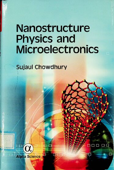
书名:Nanostructure physics and microelectronics
ISBN\ISSN:9781842659052,1842659057
出版时间:2015
出版社:Alpha Science International Ltd.,
前言
Part I This part is based on my lecture notes for courses on Microelectronics: Physics and Processing that I have been conducting for nearly a decade for 4th year B.Sc. Honours and M.S. students of Physics major. To get necessary material for the course, I needed to go through a range of books. Most books emphasize on material or microelectronic processing rather than on Physics. Lack of a book which can be used as textbook was strongly felt by students and by me as a course conductor. This book contains the course coherently as required by M.S. students of Physics. While writing this book, equal emphasis has been given to Physics and material or microelectronic processing. The book has been written in the form of lecture notes and hence teachers of courses on Microelectronics for M.S. students of Physics can use the book as lecture notes without any modification. The lecture notes of part I were compiled by my M.S. project students Syed Shafayeat Hossain, and Kazi Suffekul Islam.
Part II This part too is based on my lecture notes for a two semester M.S. course on Nanostructure Physics and Nanoelcctronics that I have been conducting for nearly a decade. This book contains course contents along with thorough discussions and extensive use of diagrams and hence this book can be used as main textbook for the course. The book has been written in the form of lecture notes and hence teachers of the course can use the book as lecture notes essentially without any modification.This is possibly the lst textbook of the course that can be used as lecture notes essentially without any modification. The entire content of the book can be covered in two semesters. I have class-tested the entire content of the book many times over a decade. No prior knowledge of the course is required. The lecture notes of part II were compiled by my M.S. project student Md. Muzammel Haque. The two parts of the textbook: Part I on Microelectronics and Part II on Nanostructure Physics should be covered as two parallel courses; understanding of part I will help achieve complete understanding of part II.
查看更多
目录
Preface v
Part I: Microelectronics: Physics and Processing
1. Semiconductor Theory 1.1
1.1 Insulator and its Band Model 1.1
1.2 Intrinsic Semiconductor and its Band Model 1.2
1.3 Extrinsic Semiconductor and its Band Model 1.4
1.4 Law of Mass Action 1.7 5
2. Introduction to Semiconductors 2.1 1
2.1 Elemental and Compound Semiconductors 2.1
2.2 Atomic Bonding in Si and in GaAs 2.4
2.3 Diamond and Zincblende Crystal Structures 2.6
2.4 Alloy Semiconductors: Ternary and Quaternary Semiconductors 2.7
2.5 Bandgap Engineering 2.9
2.6 Vegard’s Law 2.11
2.7 Substrate and Epitaxial Layer 2.11
2.8 Semiconductor Heterostructure and Heterojunction 2.12
2.9 Lattice Matched Heterostructure 2.13
2.10 Pseudomorphic Heterostructure 2.14
3. Semiconductor Crystal Growth 3.1
3.1 Bulk Single Crystal Growth of Elemental and Compound Semiconductor 3.1
3.2 Getting Pure Polycrystal of Silicon 3.1
3.3 Bridgman Method of Bulk Single Crystal Growth 3.2
3.4 Floating Zone Method of Bulk Single Crystal Growth 3.4
3.5 Czochralski Method of Bulk Single Crystal Growth 3.5
3.6 Liquid Encapsulated Czochralski (LEC) Growth of Bulk Single Crystal 3.6
3.7 Preparation of Substrate or Wafer 3.7
3.8 Epitaxial Crystal Growth 3.8
3.9 Liquid Phase Epitaxy (LPE) 3.9
3.10 Vapour Phase Epitaxy (VPE) or Chemical Vapour Deposition (CVD) 3.10
3.11 Molecular Beam Epitaxy (MBE) 3.11
4. Doping of Semiconductor Crystal 4.1
4.1 Mechanism of Free Carrier Generation by Doping in Elemental and Compound Semiconductors 4.1
4.2 Amphoteric Dopant 4-6
4.3 Intentional Doping of Semiconductor Crystal during Crystal Growth 4.6
4.4 Unintentional Doping of Semiconductor Crystal during Crystal Growth 4.6
4.5 Compensation in Semiconductor Crystal 47
4.6 Shallow and Deep Impurity Levels 48
4.7 Modulation Doping 4-9
4.8 Doping Semiconductor Crystal by Diffusion 4-10
4.9 Doping of Semiconductor Crystal by Ion Implantation 4.14
5. Theory of Junctions 5.1
5.1 p-n Junction: Electrostatics and Band Model 5.1
5.2 Rectification by p-n Junction 5.12
5.3 Metal-semiconductor Junction 5.16
5.4 Band Model of Metal-n-semiconductor Rectifying Junction: Φm > Φs 5.17
5.5 Band Model of Metal p-semiconductor Rectifying :Φm < Φs 5.18
5.6 Metal n-semiconductor Junction as a Rectifier: Φm > Φs 5.19
5.7 Metal n-semiconductor Junction: Φm < Φs Ohmic Contact5.21
5.8 Metal p-semiconductor Junction: Φm > Φs Ohmic Contact 5.23
5.9 Turning a Rectifying Metal-semiconductor Junction into Ohmic by Doping Heavily 5.24
5.10 Discrepancy between Theory and Experiment: Schottky Barrier Height does not Vary Linearly with Metal Work Function 5.24
5.11 Metallisation for Gate and for Ohmic Contact 5.29
5.12 Semiconductor Heterojunction: Band Model of Heterojunction between Two n-type Semiconductor Crystals 5.30
5.13 Band Model of Heterojunction between a p-type Semiconductor and an n-type Semiconductor of Larger Bandgap 5.32
5.14 Band Model of Heterojunction between Two p-type Semiconductor Crystals 5.34
6. Microelectronic Processing 6.1
6.1 Resist and Lithography 6.1
6.2 Positive and Negative Resist 6.4
6.3 Sensitivity, Resolution and Contrast of Resist 6.5
6.4 Optical Lithography or Photolithography 6.6
6.5 Constitution and use of Photoresist Material 6.7
6.6 Electron Beam Lithography 6.10
6.7 Proximity Effect 6.12
6.8 X-ray Lithography 6.13
6.9 Etching: Wet versus Dry Etching 6.14
6.10 Wet Etching 6.15
6.11 Plasma Etching 6.16
6.12 Ion Beam Milling 6.17
6.13 Metallisation Etching 6.18
6.14 Thermal Oxidation 6.19
6.15 CVD of Polysilicon, SiO2, and Si3N4 6.20
6.16 Physical Vapour Deposition (PVD) 6.22
6.17 Evaporation 6.22
6.18 Step Coverage 6.24
6.19 Sputtering 6.25
6.20 Metallisation for Gate and for Ohmic Contact 6.26
7. Structure and Fabrication of Some Microdevices 7.1
7.1 Fabrication of p-n Junction 7.1
7.2 Fabrication of npn Bipolar Junction Transistor (BJT) 7.3
7.3 Structure and Fabrication of MOSFET 7.5
7.4 High Electron Mobility Transistor (HEMT) 7.5
Part II: Nanostructure Physics and Nanoelectronics
8. Theories of Electron in Crystals 8.1
8.1 Nanostructure Physics and Nanoelectronics 8.1
8.2 Free Electron Theory 8.1
8.3 Bragg Reflection 8.8
8.4 Why Periodic Potential 8.14
8.5 Kronig-Penney Model: Electron in Periodic Potential 8.15
8.6 Motion of Electron in Periodic Potential: Momentum, Velocity and Effective Mass 8.21
8.7 Nearly Free Electron (NFE) Theory: Qualitative Treatment 8.24
8.8 Tight Binding Model: Qualitative Aspect 8.27
8.9 Metal, Semiconductor and Insulator: Electrical Conductivity and Band Model 8.30
9. Energy Band Structure of Bulk Real Crystals 9.1
9.1 Energy Band Structure of Real Crystals 9.1
9.2 Light Hole and Heavy Hole 9-3
9.3 Direct and Indirect Bandgap Materials 9.4
9.4 Optical Absorption and Emission 9-4
9.5 Many Valley Character of Conduction Band and Negative Differential Resistance Behavior 9.6
10. Structure, Band Model and Physics of Basic Semiconductor Nanostructures 10.1
10.1 Basic Nanostructures 10.1
10.2 Tunnel Barrier: Structure and Band Model 10.1
10.3 Quantum Well (QW) 10.6
10.4 Symmetric Double Barrier 10.10
10.5 Superlattice (1D Vertical) 10.20
10.6 Multi-Quantum Well (MQW) 10.24
10.7 p-n Junction: Electrostatics and Band Model 10.25
10.8 Doping of Semiconductor Crystal 10.39
10.9 Metal-Oxide-Semiconductor Field Effect Transistor (MOSFET) 10.48
11. Nanostructure Physics of Isolated Quantum Well in Detail 11.1
11.1 GaAs~AlGaAs Quantum Well (QW) 11.11
11.2 Electronic Structure of GaAs-AlGaAs QW 11.3
11.3 Density of Available States (DOAS) in 2D in Crystal 11.6
11.4 Density of Available States (DOAS) of QW 11.8
11.5 Occupation of Available States in QW 11.11
11.6 Optical Properties of GaAs—AlGaAs QW 11.15
11.7 Effect of Confinement of QW on Shallow Donor Level 11.19
11.8 Absorption Spectrum of Bulk Semiconductor Crystal eg. GaAs 11.20
12. Nanostructure Physics of Sawtooth and Doping Superlattices, Quantum Wire and Quantum Dot 12.1
12.1 Graded Bandgap Material and AlGaAs Sawtooth Superlattice 12.1
12.2 Doping Superlattice 12.4
12.3 Quantum Wire 12.7
12.4 Quantum Dot (QD) 12.17
13. Transport in Nanostructures 13.1
13.1 Realisation of an Electron Transmission through Rectangular and Triangular Potential Barriers 13.1
13.2 Tunnel Diode: Band Model and I-V Characteristics 13.4
13.3 Hot Electron: Velocity Overshoot and Saturation Velocity 13.8
13.4 Degenerate, Nearly Degenerate and Non-degenerate Energy Distributions of 2DEG 13.13
14. Nanostructure Physics and Nanoelectronics in 14.1
Uniform Magnetic Field
14.1 Eigenvalue Equation of Energy of an Electron in Presence of Electric and Magnetic Field 14.1
14.2 Energy Spectrum of 2DEG in ln-plane Magnetic Field 14.3
14.3 2DEG in Uniform Normal Magnetic Field: Classical Treatment 14.8
14.4 Landau Levels 14.15
14.5 Energy Spectrum and DOS of 3DEG in Uniform Magnetic Field 14.26
14.6 How to Obtain Inverse of a Matrix 14.27
14.7 Electrical Resistivity and Conductivity of 2DEG in Zero Magnetic Field: Drude Model 14.29
14.8 Shubnikov-De Haas (SdH) Oscillations or Effect 14.36
14.9 Integer Quantum Hall Effect IQHE or QHE 14.46
14.10 Fractional Quantum Hall Effect (FQHE) 14.50
14.11 Transport in Quantum Wire in Uniform Magnetic Field 14.52
15. Nanostructure Physics of MODFET in Detail 15.1
15.1 2DEG in MODFET versus 2DEG in MOSFET 15.1
15.2 Electrostatics of MODFET: Schottky Barrier 15.1
15.3 Band Model of MODFET before and after Charge Transfer 15.4
15.4 Distribution of Carriers between Surface States and 2DEG 15.7
15.5 Calculation of CB Edge Profile of MODFET 15.8
15.6 Threshold Voltage: Normally ON and Normally OFF MODFET 15.13
15.7 Etched Lateral Superlattices 15.16
15.8 Shallow and Deep Si Donor Levels in AlGaAs 15.16
15.9 Persistent Photoconductivity 15.18
15.10 Parallel Conduction 15.18
15.11 Superlattice Selectively Doped MODFET 15.18
15.12 Surface Segregation of Dopants 15.19
15.13 Raising Mobility of 2DEG to High Value 15.19
15.14 Sources of Scattering of Electrons in 2DEG 15.21
Bibliography of Part I
Bibliography of Part II
查看更多
馆藏单位
中科院文献情报中心


